
Molybdenum Round Used in Semiconductor Industry
作者:kangbote 时间:2026-05-26 17:20:16
As the semiconductor process node continues to shrink to 7nm, 5nm or even more advanced processes, as well as 3D NAND stacking, AI high-performance chips of the rapid iteration, the application of traditional metal materials short boards gradually come to the fore. High purity semiconductor-grade molybdenum disk has become a core functional material for advanced semiconductor manufacturing.
What is Molybdenum Round?
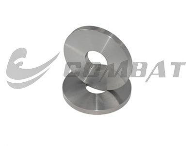
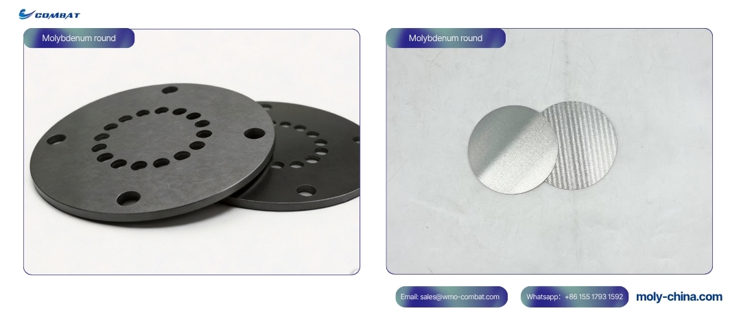
Molybdenum round, also known as molybdenum discs and round, are round, flat, precision components made from molybdenum element 42, a high-purity refractory metal product.
Unlike ordinary industrial-grade molybdenum round, semiconductor-grade products undergo rigorous purification and precision processing, with impurity content strictly controlled throughout the entire process, and can be adapted to the high-precision, high-cleanliness production environment of semiconductors.
Molybdenum Round Characteristics
Ultra-high purity, eliminating process contamination: the product purity is stable at 99.9%-99.95% and above, with extremely low metal and gas impurities, which can avoid contamination during semiconductor wafer processing and thin film deposition, and protect chip yield.
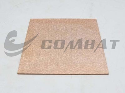
Customizable specifications, adaptable to multiple scenarios: support multi-size custom molybdenum materials, 7mm-100mm molybdenum disc diameter, 0.15mm-4.0mm molybdenum wafer thickness, and at the same time can be processed according to the need for square, ring-shaped shaped components, adaptable to the needs of different semiconductor equipment and process requirements.
Ultra-high precision machining accuracy: round flatness tolerance within ±0.01mm, surface roughness Ra <0.01μm, to meet the requirements of nanometer-scale thin film deposition and high-precision encapsulation process.
Why use Moly Round in Semiconductor Industry
Nano-scale low resistivity
Molybdenum material has a unique nanoscale conductivity advantage, and can still maintain a stable low resistivity in the ultra-thin film state. This feature can effectively increase the chip signal transmission speed and reduce the operating power consumption.
Simpler process integration
When tungsten material is used, it must be combined with TiN bonding layer, barrier layer and other auxiliary structures, which increases the coating, etching and other process steps.
The molybdenum disk supports direct deposition without a barrier layer, eliminating the need for additional auxiliary thin-film structures. ALD atomic layer deposition, CMP chemical mechanical polishing and other core processes can be greatly simplified, shortening the production process and effectively reducing the overall cost of chip manufacturing.
Extreme thermal stability
Molybdenum's melting point is as high as 2623℃, with excellent high-temperature resistance, can withstand semiconductor high-temperature annealing, deposition, etching and other process environments for a long period of time, and is not easy to be deformed and oxidized.
At the same time, its excellent thermal conductivity can quickly export the heat generated by the operation of the power chip to avoid localized heat damage to components.
Compatible with silicon-based semiconductor processes
High-purity molybdenum film can be stably deposited on the surface of silicon-based wafers, which is highly compatible with the existing semiconductor mass production process without the need for significant modification of production line equipment.
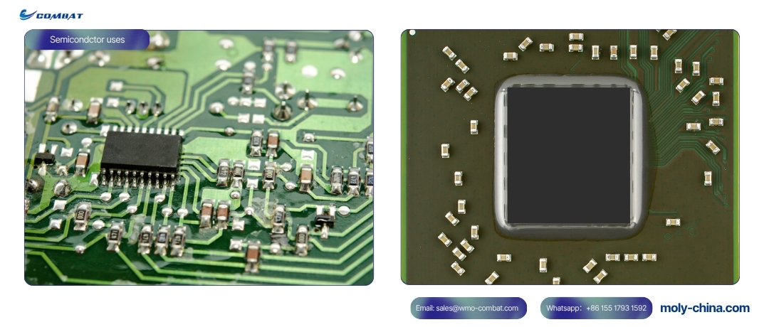
Uses of Molybdenum disks in the semiconductors
Thermal management components for power semiconductors
Molybdenum disk is the semiconductor core heat dissipation and mounting substrate, widely used in integrated circuits, large-scale integrated circuits, hybrid circuits, power transistors, diodes and other devices. It can effectively circumvent device cracking and warping problems during thermal cycling. With high thermal conductivity properties, it can quickly evacuate the operating heat of high power devices and guarantee the long-term stable work of the equipment.
High temperature and high current-carrying electrodes and conductive contacts
Molybdenum round are often used as precision conductive contacts and electrodes in power semiconductor devices such as silicon controlled rectifiers, thyristors and switchable thyristors.
In high temperature, high current working conditions, its conductive properties and mechanical structure to maintain stability, there will be no oxidation failure, deformation fracture problems, to protect the reliability of semiconductor device conductive connection.
Specialized target material for PVD sputtering coating
The molded high-purity molybdenum round can be directly used as sputtering targets for PVD physical vapor deposition, which is the core consumable for semiconductor thin film preparation.
At the same time, it is widely used in the thin film transistor process of TFT-LCD and OLED display panels, and is a key material for optoelectronic semiconductors. At present, the industry is accelerating the molybdenum metallization process to replace the traditional tungsten process, to meet the demand for small node, high-calculation power AI chip production.
Wafer carrying and precision support substrate
Molybdenum round can be used as semiconductor wafer carrier substrates, equipment mounting bases and precision support platforms.
In high-temperature processing and vacuum process, its structural dimensions are stable, no impurity precipitation, and it can accurately carry wafers and precision components, providing a stable process foundation for semiconductor processing.
Semiconductor-grade molybdenum round manufacturing
At present, there are three main processes for mass production of semiconductor-grade molybdenum round in the industry, with significant differences in finished product precision, structural stability and application scenarios.
Molybdenum bar wire cutting process
The process of molybdenum rod wire cutting molding, finished product geometric loss is small, raw material utilization rate and high yield of finished products.
Molybdenum powder direct pressure burning process
High-purity molybdenum powder is used as the raw material, and is directly pressed and sintered. The production efficiency and yield of this process are better than that of the wire-cutting process.
The shortcomings are low density, poor mechanical strength and disordered grain arrangement. When used in conjunction with silicon wafers, it is easy to crack, fracture problems, still need to continue to optimize the process parameters.
Molybdenum sheet stamping molding process
This is the current semiconductor-grade standard molybdenum disk batch manufacturing process. Relying on the uniform organizational structure of rolled molybdenum plate, together with precision stamping and polishing processing, the finished product has high density, uniform grain size and stable dimensional accuracy.
Molybdenum round technical parameters
Semiconductor grade molybdenum round can meet the needs of various high-end semiconductor equipment and processes:
Execution standard: ASTM B386
Product purity: ≥99.95% (5N high purity level)
Finished product density: >10.15g/cc, dense structure without porosity
Size range: diameter 7-100mm, thickness 0.15-4.0mm
Flatness tolerance: ±0.01mm, ultra-high dimensional accuracy
Surface roughness: Ra <0.01μm, mirror clean surface.
Molybdenum disk vs. tungsten disk in semiconductors
Molybdenum and tungsten are both refractory metal materials commonly used in semiconductors, but the two have obvious performance differences, and the applicable process scenarios have their own focus, which is the core reference for process selection.
Molybdenum disc: suitable for advanced small node chips, 3D NAND memory chips, AI computing power chip metallization and interconnect process; power semiconductor heat dissipation, device packaging, conventional high temperature process scenarios.
Tungsten round: for ultra-high temperature extreme limiting processes, special semiconductor scenarios requiring extreme thermal conductivity and ultra-high structural density.
Composite selection program: for special customized needs, can choose molybdenum-tungsten alloy, molybdenum-copper composite materials.
How to choose a high quality molybdenum disk supplier?
Semiconductor molybdenum disk directly affects the chip yield and process stability, procurement selection needs to be from the quality, qualification, capacity, service and multi-dimensional assessment, to avoid quality risks.
Verification of material quality
Priority is given to products with purity ≥99.95% and in accordance with ASTM B386 standards, and core parameters such as density, flatness and roughness of the finished product are verified. Require molybdenum metal suppliers to provide material testing reports and chemical composition analysis reports for each batch, so as to eliminate problems such as excessive impurities and dimensional deviations from the source.
Audit qualification
Regular suppliers are required to have ISO 9001:2015 quality management system certification, and their products comply with RoHS and REACH environmental compliance standards.
Examine industry experience
Priority is given to suppliers who are deeply engaged in the semiconductor industry and are familiar with the customization needs of chip coating, heat dissipation, packaging and other scenarios.
Support non-standard size, TZM, molybdenum-lanthanum alloy and other customized moly products, and can provide professional technical support for process adaptation, can solve thermal matching, process adaptation and other practical problems.
Evaluate production capacity and supply chain stability
Prefer molybdenum wafer manufacturers with integrated production capacity of sintering, rolling, machining and polishing to minimize quality fluctuations caused by outsourcing. At the same time, check the batch traceability system, delivery cycle and mass production capacity, which can be adapted to the needs of sample trial production to large-scale mass production.
Comprehensive evaluation of reputation
Refer to the supplier's customer cases in the semiconductor industry and market reputation to avoid suppliers with unstable quality and imperfect after-sales service.
Conclusion
As a high-precision molybdenum round manufacturer, COMBAT Metal focuses on the research, development and production of high-quality semiconductor-grade molybdenum round, relying on mature production processes and strict quality control system, to provide semiconductor customers with stable and reliable material solutions and full technical support.
Frequently Asked Questions of Molybdenum Round
Why is molybdenum recommended over tungsten for 10nm advanced chips?
In nanometer thin film scenarios below 10nm, tungsten material resistivity will increase dramatically, resulting in increased power consumption and decreased transmission rate. Molybdenum, on the other hand, maintains a stable low resistivity without the need for an additional barrier layer, making it a simpler process and more suitable for advanced micro node chips.
What are the purity requirements for molybdenum round in semiconductor manufacturing?
High-end semiconductor processes must use high-purity molybdenum round with a purity of ≥99.95%. Lower purity products have a high impurity content, which significantly reduces chip yields.
What is the core use of molybdenum sputtering targets in display semiconductors?
Molybdenum disk sputtering targets are mainly used for the deposition of thin film transistor conductive layers and metal wiring layers for TFT-LCD and OLED screens.
How to avoid cracking when molybdenum round are used in conjunction with silicon wafers?
Priority is given to high-purity molybdenum discs produced by the rolling and stamping process, which have uniform grains, dense structure and higher strength.
At the same time, based on the close thermal expansion coefficient of molybdenum and silicon, strict control of processing flatness and assembly process can effectively avoid cracking and warping problems during thermal cycling.