

How to Choose the Best Tungsten Copper Material for Electronic Packaging
作者:kangbote 时间:2026-07-24 10:26:23
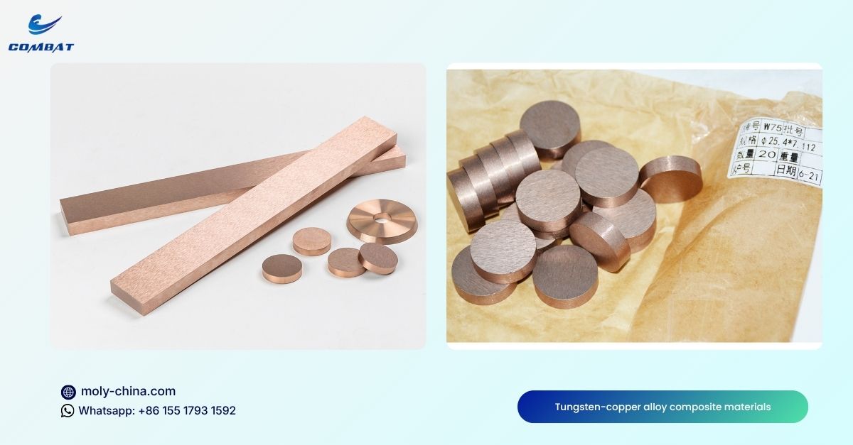
In semiconductor, power electronics, 5G RF, aerospace and other high-precision fields, electronic packaging is the core link to ensure the stable operation of chips and modules. With the continuous development of electronic equipment towards miniaturization, high power and high density integration, the working heat flux density of chips has been greatly increased, and the disadvantages of traditional packaging materials have gradually become prominent. Tungsten copper alloy (WCu/CuW composite material) has become the core material of high-end electronic packaging by virtue of its own advantages, and is widely used in core components such as heat dissipation substrates, soaking plates, package bases, lead frames, semiconductor wafers, etc. This article will help you accurately select the best tungsten copper material for your own products.
Why Tungsten Copper Is Used in Electronic Packaging?
The core technical difficulty of high-end electronic packaging is to balance the contradiction between efficient heat dissipation and thermal deformation matching. Traditional materials such as pure copper, kovar, molybdenum copper, and silicon carbide aluminum each have shortcomings in performance. It is difficult to balance high-power heat dissipation with structural stability, and cannot adapt to the harsh working conditions of precision electronics.
The tungsten-copper material relies on the complementary properties of copper and tungsten to achieve a golden balance between thermal conductivity and thermal expansion coefficient. The copper component is responsible for quickly deriving the working high temperature of chips, IGBTs and RF devices, while the tungsten component provides extremely low thermal expansion coefficient, which can accurately match semiconductor substrates such as silicon, gallium arsenide and ceramics, effectively avoiding package failure caused by thermal stress.
In addition to excellent thermal properties, tungsten copper also has excellent mechanical stability and comprehensive compatibility. Its tensile strength can reach 500 - 800MPa, high hardness, good rigidity, not easy to deform and crack under long-term high and low temperature cycles, vibration and impact conditions, which can stably guarantee chip bonding and airtight packaging effect. Compared with all kinds of traditional materials, tungsten copper has remarkable comprehensive performance advantages, and is the preferred material for 5G, aerospace, military, high-power semiconductor and other high-reliability electronic packaging scenarios.
What Properties Matter Most When Choosing Tungsten Copper?
In our many years of industry experience, tungsten copper material is not a universal material, there is no optimal grade. All properties are dynamically adjustable around the tungsten copper ratio. The core logic of selection is: balance thermal conductivity, thermal expansion matching, mechanical strength and processing performance according to product conditions.
1. Tungsten copper ratio
Tungsten copper ratio (tungsten copper mass ratio) is the core decisive factor of all properties, and it is also the first step of selection. Tungsten and copper are almost insoluble, forming pseudo-alloy composites. The ratio change will directly rewrite all key properties such as thermal conductivity, expansion, strength and processing of the material.
High tungsten low copper ratio (such as W85Cu15, W90Cu10): the core advantage is lower thermal expansion coefficient, higher density, better hardness and structural strength, thermal fatigue resistance, arc erosion resistance. However, the corresponding thermal conductivity and electrical conductivity will decrease slightly, and the material processing difficulty will also increase slightly.
High copper and low tungsten ratio (such as W70Cu30, W75Cu25): The core advantages are full thermal and electrical conductivity, better material toughness, excellent machining performance, and can be adapted to complex structure processing. However, the short board has a high thermal expansion coefficient, and the matching degree with the semiconductor substrate will be reduced.
For conventional electronic packaging scenarios, the industry mainstream selects W80Cu20 and W75Cu25 for two large and medium balance ratios, which can not only meet the requirements of efficient heat dissipation, but also ensure accurate thermal expansion matching, and adapt to most power semiconductor and RF device packaging scenarios.
2. Thermal performance
Thermal performance is the core evaluation index of electronic packaging tungsten copper material, which directly determines the heat dissipation efficiency and long-term operation reliability of the device, mainly including thermal conductivity (TC) and thermal expansion coefficient (CTE).
Thermal conductivity determines the heat dissipation ability of the device, and directly affects the temperature rise and power load limit of the chip.
The thermal conductivity range of tungsten copper materials is stable at 170 - 230W/m·K. The higher the copper content, the better the thermal conductivity. For GaN, IGBT and other high power devices, high copper ratio materials should be selected first to avoid overheating failure caused by heat accumulation.
Thermal expansion coefficient determines the stability of package structure, which is the key to prevent cracking, delamination and desoldering. The coefficient of thermal expansion of semiconductor silicon substrate is only 2 - 4ppm/℃, and that of ceramic substrate is about 4 - 8ppm/℃. When selecting, it is necessary to ensure that the difference between CTE of tungsten copper material and substrate is controlled within 1 - 2ppm/℃.
CTE of tungsten copper material with high tungsten ratio can be as low as 6ppm/℃, which can achieve the ultimate substrate matching, suitable for aerospace, high-end RF and other scenarios with high reliability requirements. At the same time, tungsten's ultra-high melting point makes the material have excellent high temperature thermal stability and can withstand high and low temperature cyclic shocks for a long time.
3. Mechanical properties
Electronic packaging devices are often faced with equipment vibration, temperature alternation, mechanical shock and other conditions, the mechanical properties of materials directly determine the service life of packaging structures. Tungsten copper relies on tungsten hard skeleton structure, with excellent comprehensive mechanical properties.
The overall tensile strength of the material can reach 500 - 800MPa, with high hardness and rigidity, and it is not easy to plastic deformation. In the long-term thermal cycle process, the flatness of the packaging substrate and the base can be continuously maintained, and the bonding failure and airtightness failure problems caused by warpage and deformation can be avoided.
At the same time, compared with pure tungsten materials, tungsten copper composite materials have better toughness and are not easy to crack, taking into account high strength and good processing adaptability, which can meet the production requirements of precision thin sheets, irregular structures and high-precision planar packages.
Tungsten copper grades in different industries
Standardized tungsten copper alloy grades on the market are all distinguished by the ratio of tungsten to copper. The performance focus and adaptation scenarios of different grades vary greatly. There is no universal optimal brand, only the most suitable choice for the appropriate working conditions. The following are the accurate selection solutions for mainstream brands in the field of electronic packaging.
- W90Cu10 core performance: CTE as low as 6.0 - 6.5ppm/℃, structural strength, hardness, density industry top, excellent thermal fatigue, arc corrosion resistance, thermal conductivity 170 - 200W/m·K. Adapted scenarios: aerospace, military-grade high-reliability electronic packaging, ultra-high precision RF devices, radiation shielding packaging components, suitable for extreme thermal deformation control scenarios.
- W85Cu15 core performance: CTE 6.5 - 7.5ppm/℃, thermal conductivity 180 - 210W/m·K, both ultra-low thermal expansion and excellent heat dissipation performance, comprehensive stability is extremely strong. Adaptation scenarios: 5G base station RF module, GaN high power chip, laser device package, high-end industrial power module, is the preferred brand of high reliability high-end package.
- W80Cu20 core performance: CTE 7.0 - 8.0ppm/℃, thermal conductivity 190 - 220W/m·K, thermal matching and heat dissipation performance perfect balance, high cost performance. Adaptation scenarios: Most conventional semiconductor packages, IGBT power modules, LED high-end packages, and ordinary RF devices are common reference brands for civil and industrial electronic packages.
- W75Cu25 / W70Cu30 core performance: thermal conductivity up to 200 - 240W/m·K, thermal conductivity full, excellent processability, toughness, CTE 8.0 - 9.5ppm/℃. Adaptation scenarios: ultra-high heat flux, extreme heat dissipation requirements of the packaging scenarios, suitable for heat dissipation priority over thermal expansion matching devices, such as high-power heat dissipation soaking plate, universal heat dissipation base.
Manufacturing process determines actual performance
The vast majority of errors in selection have the same problem: that the same proportion of tungsten copper materials, the performance is completely consistent. In fact, tungsten copper belongs to powder metallurgy composite materials, tungsten copper immiscible characteristics, so that the manufacturing process directly determines the actual quality of the material, the process gap is much greater than the nominal difference.
Simply put: the ratio determines the upper limit of the theoretical performance of the material, and the manufacturing process determines the actual performance of the material. For the same W80Cu20 material, the finished products produced by different processes may have a difference of more than 30% in thermal conductivity, porosity and service life.
Infiltration method
Infiltration method is the preferred manufacturing process for tungsten copper materials for high-end electronic packaging, especially suitable for W80Cu20, W85Cu15, W90Cu10 and other high tungsten and low copper grades.
The process principle is to press and pre-sinter to form porous tungsten skeleton, and then infiltrate molten copper into the pores of tungsten skeleton by capillary action under high temperature vacuum or hydrogen atmosphere. The process can achieve high density of more than 99%, extremely low porosity, uniform distribution of copper, and continuous and stable thermal conduction network.
The tungsten-copper material produced by the infiltration method has stable thermal conductivity, accurate thermal expansion coefficient, strong interface adhesion, and excellent thermal cycle fatigue life. It can perfectly adapt to the high reliability requirements of precision electronic packaging and is recognized as the best process solution in the industry.
Standard VS Custom Tungsten Copper Alloy: How to Choose?
In the process of electronic packaging project landing, many engineers will be entangled in the selection: is it directly to choose the spot standard brand, or to invest in the cost of custom tungsten copper materials? There is no absolute advantage or disadvantage between the two, the core depends on product conditions, mass production scale, reliability requirements and cost budget.
1. Preferred selection of standard tungsten copper composite materials
Standard grades (W70Cu30, W75Cu25, W80Cu20, W85Cu15, W90 Cu10) are mature formulas in the industry, with large-scale mass production, sufficient inventory, short delivery time and controllable cost.
These materials have complete test data, industry standard certification (ASTM B702), mass market verification, stable reliability, early product certification, and shorter test cycles.
Suitable for conventional power electronics, general RF devices, small and medium batch production, project cycle tight scenarios. Most civilian and industrial-grade electronic packaging projects rely on standard W80Cu20 and W85Cu15 to meet all performance requirements without additional customization.
2. Application of customized tungsten copper
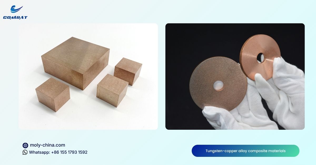
Customized tungsten copper alloy component includes personalized tungsten copper ratio, functionally graded materials (FGM), shaped near net shape, special surface treatment, ultra-low porosity customization and other solutions, mainly suitable for high-end extreme conditions.
When the product needs extremely accurate CTE substrate matching, ultra-high heat flux heat dissipation, extreme high and low temperature cycle conditions, or aerospace, high-end medical, and other mission-critical scenarios, the standard brand will have short performance, and the advantages of customized materials will be completely highlighted.
Gradient customized materials can achieve "high copper in the surface layer to improve welding thermal conductivity, high tungsten in the core to ensure structural strength and low expansion", perfectly solve the performance contradiction of a single material, and greatly improve the service life and stability of the device.
Guide to Avoiding Mistakes When Selecting Tungsten-Copper Materials
Combined with industry engineering experience, most electronic packaging tungsten copper failure problems, not the wrong material brand selection, but the details of the selection, procurement, verification link errors. The following eight high-frequency errors are the core minefields that R & D and procurement must avoid.
- Only look at the ratio, ignore the manufacturing process Many people blindly recognize W80Cu20 and other high-quality brands, but ignore the process differences. Sintering process of the same proportion of materials, high porosity, uneven structure, easy to appear poor heat dissipation, thermal cycle failure, can not replace the infiltration process products.
- Only refer to room temperature parameters, ignoring high temperature conditions performance manufacturers parameter table is mostly room temperature test data, but power electronics long-term work at 100 - 200℃ high temperature, material thermal conductivity, CTE, strength will change slightly. Only referring to room temperature data will lead to thermal mismatch and insufficient heat dissipation under actual conditions.
- Ignoring the surface accuracy and post-treatment adaptability package bonding, airtight packaging on the material surface flatness, roughness requirements are extremely high. Rough surface, flatness will increase the interface thermal resistance, causing voids, false welding, delamination failure, need to be clear in advance Ra roughness, flatness, plating adaptation requirements.
- Blind pursuit of high thermal conductivity, ignoring CTE matching blindly choose high copper high thermal conductivity brand, will lead to high thermal expansion coefficient, and silicon, ceramic substrate mismatch. Under long-term temperature cycling, thermal stress accumulates continuously, resulting in device cracking and solder joint fatigue failure.
- Standard and custom selection of the cart before the horse conventional conditions blindly customized materials, will greatly increase the cost, lengthen the delivery period; extreme severe conditions using standard grades, will lead to insufficient product reliability, after-sales failure rate soaring.
- Ignoring the porosity and microstructure of the nominal ratio of qualified materials, if the porosity exceeds the standard, copper phase segregation, there will be local uneven performance. These hidden defects are not exposed in routine testing and only focus on failure under long-term thermal cycling conditions.
- Skip sample verification and reliability test completely rely on the manufacturer's data manual, do not do sample measurement, thermal cycle test, power aging test, can not check the hidden quality problems of materials, it is easy to appear batch failure risk after mass production.
- Only compare the unit price, ignore the comprehensive cost of low-quality tungsten copper material seems to save procurement costs, but will increase the product failure rate, after-sales costs, rework costs. High quality tungsten copper material has stable performance, longer life and lower comprehensive cost in the whole life cycle.
How to select reliable tungsten copper suppliers for electronic packaging?
The core of material selection is half of the selection of brands and half of the selection of suppliers. The process control, testing ability and technical service of high-quality suppliers directly determine the batch consistency of materials and the final reliability of products. For tungsten copper supplier screening, please refer to the following core criteria.
- Check the core process capability.
Preference should be given to manufacturers with mature infiltration process production capacity, which can stably produce electronic grade tungsten copper materials with more than 98% density and low porosity. Refuse low-end products without process control and only powder sintering, and confirm that the manufacturer can provide microstructure and porosity test reports.
- Verification of complete quality inspection system.
Regular suppliers can provide relevant inspection data reports to support third-party retest. At the same time with ISO9001, IATF16949, AS9100 and other industry certification.
- Matching electronic packaging industry experience.
Priority is given to suppliers who are deeply involved in semiconductor, power electronics and RF packaging, familiar with packaging process requirements, and have relevant industry cases and customer endorsements.
- Customization and mass production capacity.
High-quality suppliers can provide standard spot and customized services at the same time, support mass production, stable delivery, strong batch consistency, can optimize material parameters and processing technology according to customer needs.
- Transparent price.
Rejection of low-cost inferior tungsten copper material cost and process, raw material purity is strongly related, abnormal low-cost products must have process shrinkage, raw material impurity, porosity and other problems. Reliable supplier quotation transparent, can clearly distinguish the price difference of standard products, customized products and different process products.
Frequently Asked Questions
Q: Tungsten copper and molybdenum copper which is more suitable for semiconductor packaging?
Tungsten copper alloy is preferred for high-end, high-reliability semiconductor packaging. Tungsten copper has higher thermal conductivity, stronger structural stability and better thermal fatigue resistance; molybdenum copper is lighter, suitable for lightweight, low power and conventional heat dissipation scenarios, and its performance under high power conditions is inferior to tungsten copper.
Q: which kind of tungsten copper brand thermal conductivity is best?
Under the same process conditions, the higher the copper content, the better the thermal conductivity. W70Cu30 has the best thermal conductivity, followed by W75Cu25 and W80Cu20. High thermal conductivity grades are suitable for ultra-high heat flux heat dissipation scenarios.
Q: What tungsten copper brand best match silicon substrate?
The CTE of silicon substrate is 2 - 4ppm/℃, preferably W85Cu15 and W90Cu10, and the difference of thermal expansion coefficient is very small, so that the thermal stress can be reduced to the greatest extent, and the problem of cracking and layering can be avoided.
Q: Tungsten copper CNC precision machining can do?
Very good. The tungsten copper alloy can realize high-precision CNC milling, grin and punching, has high machining precision and good surface flatness, and that machining performance is far superior to that of pure tungsten, and can meet the requirement of a miniaturized and precise electronic packaging structure.
Q: Tungsten copper support nickel gold plating process?
High quality infiltration tungsten copper material has extremely low porosity, compact and uniform surface, which can perfectly adapt to surface treatment processes such as chemical nickel and gold plating. The coating has strong adhesion and no bubble cavity, which meets the requirements of packaging, welding and corrosion prevention.
Q:Infiltration of electronic grade tungsten copper standard density is how much?
According to different grades, the density range is 12-17g/cm³, with W90Cu10 having the highest density and W70Cu30 having the lowest density. The density of regular infiltration products can reach more than 99%.
Q: Tungsten copper is suitable for high power semiconductor packaging?
It fits perfectly. With high thermal conductivity, precise CTE matching, high mechanical stability and long fatigue life, tungsten copper is the core standard material for the third generation semiconductor high power packages such as IGBT, GaN and SiC.
Q: What is the service life of tungsten copper under high power conditions? Tungsten copper with high quality infiltration technology can realize stable operation of more than 100,000 times of thermal cycles under the working conditions of conventional high and low temperature cycles and continuous high power, without deformation, cracking and failure, and its service life is far longer than that of ordinary packaging alloy materials.
Conclusion
Choosing the right tungsten copper material is not only about selecting an alloy grade. It also involves understanding thermal management requirements, manufacturing quality, and long-term application reliability. Working with an experienced manufacturer can help optimize both product performance and total lifecycle cost. At COMBAT, we believe every electronic packaging project has unique thermal and mechanical requirements. By combining material expertise with precision manufacturing, we help customers select tungsten copper solutions that balance performance, reliability, and cost-effectiveness.