

Why Tungsten and Molybdenum Matter in Semiconductor Industry
作者:kangbote 时间:2026-07-27 17:23:58
When it comes to the semiconductor industry, the public's attention is always focused on silicon wafers, EUV lithography, copper interconnection, and AI acceleration chips. Few people have noticed the role of refractory metal materials in the semiconductor industry. Tungsten (W) and molybdenum (Mo) form the core of this material system, carrying the conductive structure at the nanoscale inside the chip.
As the transistor enters the era of surround gate (GAA), the 3D stacked chip and the back power supply architecture are gradually implemented. AI computing power chips continue to increase the current density, and the characteristic size of the device continues to shrink. At this time, contact resistance and RC delay are no longer secondary issues, which directly limit chip performance, power consumption and integration density.Tungsten and molybdenum rely on ultra-high melting point, stable heat resistance, and anti-electromigration ability to solve the insurmountable nano-manufacturing problems of silicon, aluminum, and copper.
What is a refractory metal? Detailed introduction
In the industry definition, metals with melting points generally higher than 2000℃ are collectively referred to as refractory metals. The mainstream categories include tungsten, molybdenum, tantalum, niobium, and rhenium. Among them, tungsten, molybdenum, and tantalum have been commercially used on a large scale in wafer manufacturing.
This kind of material has a unique set of comprehensive properties and is suitable for harsh chip process environments:
- Ultra-high melting temperature, can withstand high temperature processes such as annealing and film deposition, and will not soften and deform.
- The coefficient of thermal expansion is matched with silicon and dielectric materials to reduce the risk of stress and warping caused by the thermal cycle.
- Excellent anti-electromigration performance, suitable for high-density chip internal high-current continuous transmission conditions.
It supports CVD and ALD conformal film deposition to achieve high aspect ratio and no gap filling of tiny holes.
In the plasma and chemically corroded wafer process environment, it has excellent chemical stability.
There is a clear division of labor at the material level inside the chip.Silicon is responsible for the construction of active transistor devices; copper is responsible for the global interconnection of medium and long distances. Tungsten and molybdenum are responsible for the contact holes, through holes, and local interconnection structures closest to the transistor and the smallest size. Without such refractory metals, the nanoscale conductive path of advanced node chips cannot be stably realized.
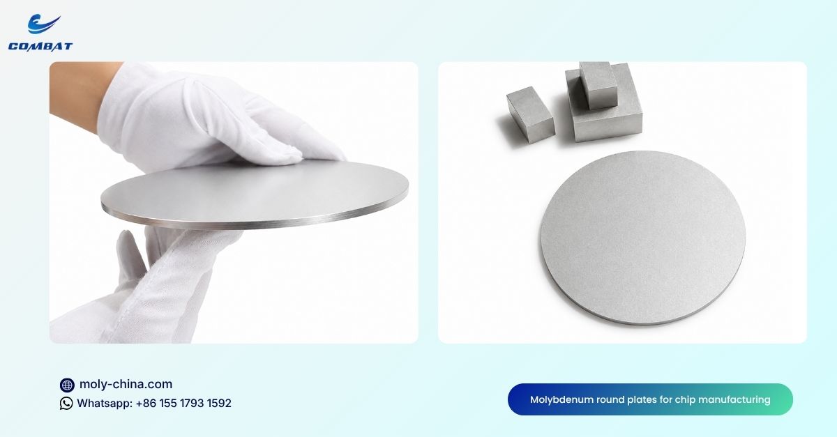
Tungsten: traditional metal material for semiconductor manufacturing
Advantages of tungsten in semiconductor manufacturing
Tungsten has the industry's top melting point of 3422℃, and its thermal stability is outstanding among commercial conductive metals. Relying on the chemical vapor deposition process of tungsten hexafluoride (WFCS), the conformal filling capacity of the film has been verified for a long time. Even in the face of a high aspect ratio structure with large depth and small aperture, no hole filling can still be achieved. COMBAT's decades of experience in large-scale mass production have made Tungsten's complete integrated process mature and stable, and it can stably supply fab materials.
Application of tungsten in semiconductor field
1.Transistor contact plug
This is the most classic and widely used scenario of tungsten. Fill the contact holes of the source, drain, and gate of the transistor to build a conductive channel between the transistor and the upper metal layer. The vast majority of mature and mid-range process nodes continue to adopt tungsten contact plug solutions.
2.Local through hole and midline interconnection
Tungsten is used to connect the local through holes of the upper and lower metal layers, concentrated close to the underlying wiring area of the transistor. At very small sizes, the barrier layer required for copper will take up a lot of space, and the use of tungsten material used to be a more cost-effective choice.
3.Memory-related structure
DRAM buried word lines, 3D NAND internal contact holes, and metal grids are filled with a lot of tungsten. Stacked 3D NAND has a large number of towering narrow and long channels, and its excellent filling capacity supports the landing of early multi-layer stacking solutions.
4.High-purity tungsten sputtering targets and equipment parts
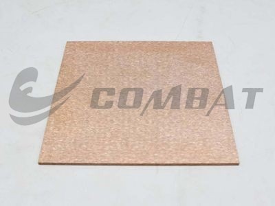
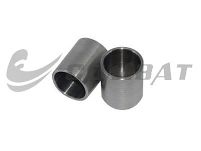
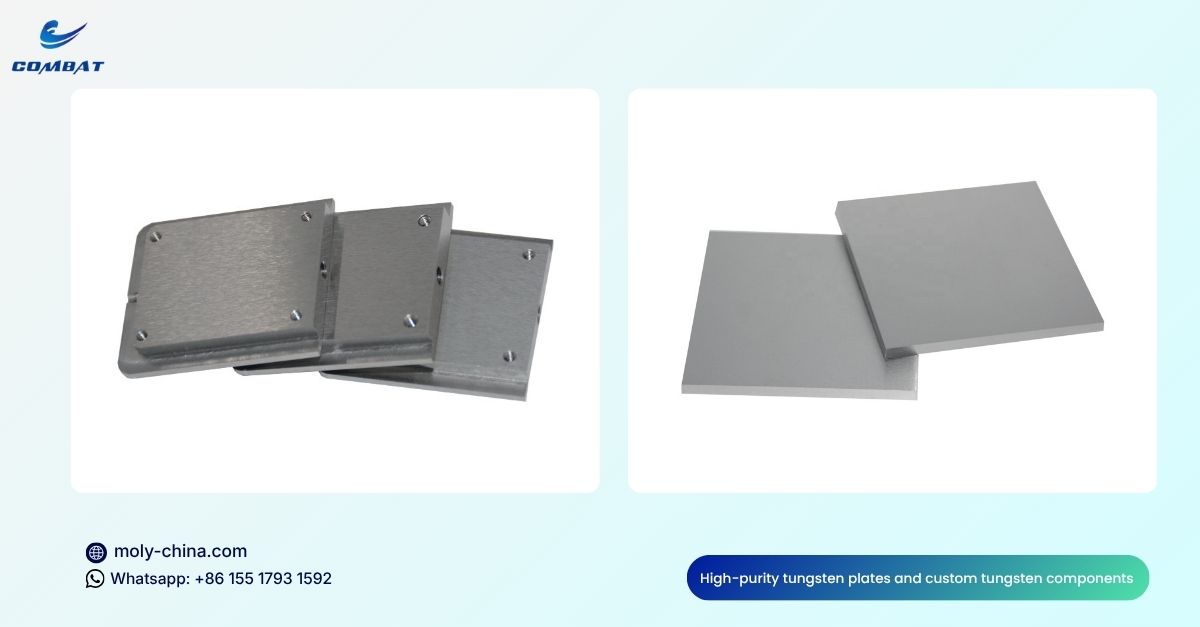
High-purity tungsten sputtering targets are used to deposit barrier layers and electrode films. At the same time, high-purity tungsten plate is widely used in high-temperature components inside wafer equipment: heaters, long-crystal crucibles, plasma shielding parts, and furnace body structural parts.
Physical bottlenecks encountered by tungsten in advanced processes
When the process advances to advanced nodes of 7nm and below, the shortcomings of tungsten gradually become prominent. When the thickness of the film is reduced to the nanometer level, the electron scattering effect intensifies and the resistivity of the film increases significantly.
The tungsten deposition process is generally equipped with a TiN barrier / liner layer. Within a very small characteristic size, the barrier layer will occupy a large cross-sectional area, compressing the effective conductive area. At the same time, the WF3 precursor releases fluorine residues, which can easily erode the surrounding dielectric layer and bring the risk of process defects.
After the current density continues to increase, the hidden dangers of tungsten's electromigration continue to increase. Many fabs began to look for alternative materials, and the commercialization process of molybdenum accelerated.
Molybdenum: material for next-generation chips
Competitive advantage of molybdenum over tungsten
At the same nano-thin film scale, the resistivity of molybdenum thin film can be reduced by up to 30%, effectively reducing RC delay and power consumption loss. Molybdenum has a low diffusion coefficient, and many scenarios can achieve barrier-free layer integration. After eliminating liners such as TiN, the proportion of conductive areas increases, while simplifying the entire deposition process.
The average free path of molybdenum electrons is shorter, and the environmental adaptability of ultra-thin films below 7~10nm is stronger. It supports selective ALD and cyclic deposition processes, which can accurately regulate the grain size and continuously depress the thin film resistance. The deposition route can avoid the fluoride precursor and eliminate the classic problem of fluoride ion corrosion of the dielectric layer.
Global equipment manufacturers continue to promote the adaptation process, represented by Panlin ALTUS series ALD equipment. Molybdenum metallization solutions have gradually moved from laboratory research and development to mass production lines for memory and advanced logic chips.
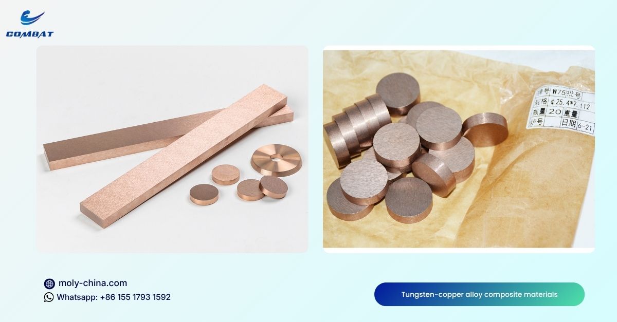
Application of molybdenum in semiconductor industry
1.Advanced logic GAA transistor contact hole, local interconnection
For AI and HPC high-end chips, molybdenum is generally used for surround gate transistor to build the underlying conductive path. At the same time, molybdenum is a candidate material with great potential for high-density power supply networks to meet the needs of high-density power supply.
2.3D NAND and DRAM word line
Storage manufacturers are the first players in China to land on a large scale.The use of molybdenum to make word wires can reduce the line width and increase the density of the memory cell while maintaining the same resistance. Industry test data show that the solution can achieve a 7% line spacing reduction and an overall storage density increase of more than 15%. It is also a key material solution for the continuous iteration of thousand-level 3D NAND.
3.High-purity molybdenum sputtering target material and thermal management components
High-purity molybdenum targets are used for depositing electrodes, adhesive layers, and advanced packaging conductive films. The coefficient of thermal expansion of molybdenum matches silicon, and it is widely used as a power semiconductor substrate, a heating plate, and a heat dissipation substrate.
Molybdenum industry landing status quo
Molybdenum no longer stays in the laboratory verification stage, and officially enters the mass production climbing cycle. However, the complete set of ALD deposition precursor, process parameters, and yield control system is still being continuously optimized. At this stage, many factories adopt the idea of mixed metallization: tungsten is retained in the mature layer, and molybdenum is used in the most advanced local interconnection.
Tungsten VS Molybdenum: how semiconductor engineers choose right material
Comparison of key performance parameters
|
Property |
Tungsten (W) |
Molybdenum (Mo) |
|
Melting point |
3422 °C |
2623 °C |
|
Thin-film resistivity (nanoscale) |
Higher |
Up to 30% lower than tungsten |
|
Barrier/liner requirement |
TiN adhesion/barrier layer usually required |
Capable of barrierless integration in most scenarios |
|
Process maturity |
Over 20 years of high-volume manufacturing (HVM) validation |
Rapidly maturing for leading-edge advanced nodes |
|
Machinability |
High hardness, strong brittleness, extremely difficult to machine |
Better machinability than tungsten, still categorized as difficult-to-process refractory metal |
Scenes where tungsten is preferred
The production line is running mature and mid-range process nodes, and they do not want to take the risk of brand-new process transformation. There is an extremely high temperature process link inside the device, which needs to maximize heat resistance stability. It is necessary to fill ultra-high aspect ratio contact holes, relying on the excellent filling capacity of traditional WFD-CVD. Tungsten is preferred for high-temperature structural parts and plasma straight-face parts of semiconductor equipment.
Give priority to molybdenum scenarios
Development of advanced logic chips below 10nm, GAA architecture, and AI computing power chips. The goal is to reduce the contact resistance, reduce power consumption, and pursue a higher chip operating frequency. 3D NAND, a new generation of DRAM, needs to reduce the word-line spacing and increase the storage density. Layout, power supply, 3D heterogeneous integration and other next-generation chip architectures.
Manufacturing difficulties faced by high-purity tungsten and molybdenum parts
In COMBAT, our many years of manufacturing experience have shown that tungsten and molybdenum have ultra-high melting points and cannot be produced by conventional melt casting processes.The vast majority of parts rely on powder metallurgy, hot isostatic pressing and sintering to achieve densification and molding.
Problems of blank preparation and purity control
Sintering requires vacuum or hydrogen to protect the high-temperature furnace, and energy consumption is expensive. Oxygen, carbon, and nitrogen impurities can easily gather at the grain boundary, causing the material to become brittle. Semiconductor-grade products require impurity control to reach the ppb level, and the control threshold is much higher than that of general industrial components.
Even if the sintering is completed, the porosity, grain size, and grain orientation still need to be precisely regulated. Especially for sputtering targets, the microstructure directly affects the level of particle defects in wafer production.
Precision machining challenges
Under room temperature conditions, the plasticity of the two materials is poor, and they are prone to chipping and cracking. Tungsten processing is the most difficult, ordinary tools wear out extremely quickly, and EDM and grinding are generally used. Molybdenum has better processing performance than tungsten, but it is still prone to work hardening and surface burrs. The scrap rate of complex, thin-walled and special-shaped parts processing is high, which pushes up the cost of finished products.
Risk of high temperature oxidation
When the temperature rises above 400~500℃, tungsten and molybdenum oxidize rapidly in the air. Molybdenum will generate volatile molybdenum trioxide, which will continue to erode the surface of the workpiece. All high-temperature processes such as sintering, welding, and annealing must be isolated from air. During the long-term storage of finished products and the service phase of equipment, it is also necessary to control the use environment to prevent oxidation and failure.
Unique challenges of thin film deposition process
Tungsten: Mature technology, but fluorine residual defects persist, and the space occupied by the barrier layer cannot be avoided. Molybdenum: The development of ALD precursor is difficult, and the stress and grain uniformity of the film need to be strictly controlled. Both materials need to be matched with supporting etching and CMP chemical mechanical polishing processes, and the entire development cycle is long.
How do semiconductor companies choose reliable tungsten and molybdenum suppliers?
Material purity and micro-consistency directly affect wafer yield, and price should not be used as the first criterion for judgment. The procurement of tungsten and molybdenum parts and sputtering targets in the semiconductor field requires the establishment of a complete evaluation system.
Verification of purity testing and quality control capabilities
Confirm that the supplier can provide the corresponding semiconductor grade products (99.95%, 5N, 6N high purity specifications). Request a complete analysis report, focusing on the content of oxygen, carbon, nitrogen and various metal impurities.
Investigate integrated manufacturing capabilities
The ideal tungsten supplier has a complete industrial chain: powder preparation → pressing molding →sintering / HIP densification → precision machining → clean cleaning. Simple traders lack process control capabilities, making it difficult to stably supply semiconductor-grade targets and precision parts.
Focus on confirming whether manufacturers have actual cases of serving fabs and semiconductor equipment OEMs. Can special-shaped parts and special-size sputtering targets be customized according to the drawings to achieve precise tolerance control.
Qualification, traceability and supply chain stability
The basic qualifications meet at least ISO9001, and the AS9100 system can be used for high-end manufacturing. A complete batch traceability system, the whole process from raw materials to finished products is recorded to facilitate the reverse investigation of defects.
At the same time, supply chain risks need to be assessed.The origin of tungsten and molybdenum raw materials is concentrated, and it is recommended to evaluate the supplier's inventory planning and delivery control capabilities. Manufacturers with export compliance experience and smooth completion of cross-border supply are more suitable for overseas wafer projects.
Technical capabilities
High-quality tungsten and molybdenum suppliers not only ship, but also provide material selection suggestions and manufacturability optimization solutions. When encountering film defects and cracking problems of parts and components, failure analysis can be carried out in collaboration.
Whole life cycle cost of tungsten and molybdenum
Low-cost tungsten and molybdenum materials, once the wafer batch defect is caused, the loss will far exceed the material difference. Evaluating costs requires comprehensive yield, scrap rate, delivery stability, and after-sales technical support. It is recommended to carry out parallel sample tests in the early stage to verify the consistency of the products of multiple suppliers, and then introduce mass production.
Frequently Asked Questions
Q1: What purity grades of tungsten and molybdenum are required for semiconductor applications?
A: General equipment structural parts are commonly used with 99.95% purity. Used in high-end scenarios of sputtering targets and thin film deposition, 5N (99.999%) or even 6N ultra-high purity specifications are generally required. The impurity content needs to be strictly controlled for oxygen, carbon, and nitrogen. Trace impurities will increase the resistance of the thin film and induce wafer defects.
Q2: Can manufacturers customize tungsten and molybdenum parts according to semiconductor equipment drawings?
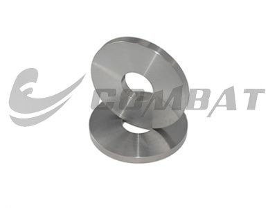
A: Professional tungsten and molybdenum component manufacturers with powder metallurgy integration capabilities support full customization. It includes all kinds of tungsten plates, bars, crucibles, shielding parts, special-shaped sputtering targets, and EDM finishing parts. Customized orders need to confirm tolerances, surface roughness, cleanliness, and packaging requirements.
Q3: Why are refractory metals better than aluminum and copper for the underlying contact structure?
A: The coverage capacity of aluminum steps is poor, and the electromigration is serious, and it cannot be adapted to a very small size structure. The copper body has excellent electrical conductivity, but it must be equipped with a heavy tantalum barrier layer. At the bottom of the nano-layer, the barrier layer occupies most of the space, greatly weakening the performance advantages of copper. Tungsten and molybdenum take into account heat resistance, diffusion resistance, and conformal filling, which just matches the requirements of the underlying conductive structure.
Q4: What factors affect the price of tungsten and molybdenum semiconductor parts?
A: The price of raw materials, the target purity level, the micro-performance requirements, the difficulty of processing, and the quantity of orders will all affect the quotation. High-purity target materials require additional densification and clean processing, and the cost is much higher than that of ordinary industrial plates.
Q5: Will molybdenum completely replace tungsten semiconductor metallization applications in the future?
A: Comprehensive substitution will not be achieved in the short and medium to long term. Tungsten still has irreplaceable advantages in ultra-high heat resistance scenarios and mature node high aspect ratio filling. The industry is moving towards a mixed metallization route where tungsten and molybdenum coexist, and it is flexibly selected according to the process node and device structure.
Conclusion
It is difficult for ordinary people to see tungsten and molybdenum on the appearance of the chip, but the two form the core channel of electronic transmission inside the chip. Tungsten relies on mature technology to protect the stable operation of a large number of mature process production lines around the world. Contact us if you are looking for tungsten and molybdenum material for semiconductor industry.